
Are you involved in the electronics industry? If so, get ready for a game-changing shift in printed circuit board (PCB) demand! As our gadgets get smaller, thinner, and lighter, the PCB world is evolving. Multilayer and high-density interconnect (HDI) PCB technologies are taking center stage. Let’s dive into what this means for you and the market.
The Driving Forces Behind PCB Evolution
1. Miniaturization: Small is the New Big
Remember when bigger meant better? Those days are gone! Now, it’s all about packing more power into smaller packages. From smartphones to smartwatches, devices are shrinking, but their capabilities are expanding. This miniaturization trend is pushing PCB technology to new heights.
2. Complexity: More Features, More Challenges
Today’s devices aren’t just smaller; they’re smarter too. Think about your phone – it’s a camera, computer, and communication device all in one. This increased functionality demands more complex PCB designs, capable of supporting multiple features in a compact space.
3. Government Initiatives: Bringing PCB Production Back Home
The U.S. government is making big moves to boost domestic PCB production. In 2023, they authorized the use of the Defense Production Act Title III. What does this mean? More money and support for U.S.-based PCB manufacturers. The Department of Defense (DoD) is nearly doubling its budget for PCBs and packaging, from $43 million in 2023 to a whopping $85.76 million in 2024.
4. Consumer Demand: The Market is Booming
People can’t get enough of the latest tech gadgets. This skyrocketing demand is pushing manufacturers to innovate and produce more advanced PCBs at a faster rate.
The Rise of Multilayer and HDI PCBs
What are Multilayer PCBs?
Imagine a PCB sandwich – that’s essentially what a multilayer PCB is. It’s multiple layers of circuitry stacked together, allowing for more complex designs in a smaller space. As devices get more sophisticated, multilayer PCBs are becoming the go-to solution.
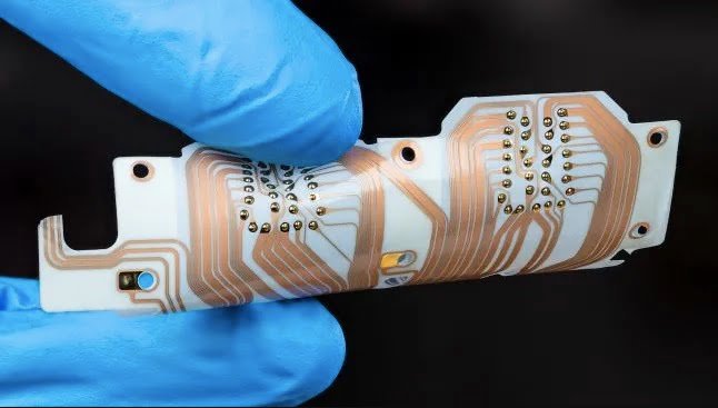
HDI PCBs: The Future is Here
High-Density Interconnect (HDI) PCBs take things a step further. They pack even more circuitry into an even smaller area. How? By using advanced techniques like microvias and finer lines and spaces. HDI PCBs are the secret sauce behind ultra-thin smartphones and other compact devices.
Market Trends: Numbers Don’t Lie
Let’s talk numbers. The HDI PCB market is set to explode:
- 2023 value: $12.45 billion
- 2030 projected value: $25.42 billion
- That’s a growth of $12.97 billion in just 7 years!
- Compound Annual Growth Rate (CAGR): 10.6%
But wait, there’s more! Flexible PCBs are also on the rise:
- 2022 market value: $19.7 billion
- 2032 projected value: $56.7 billion
- CAGR: 11.2%
These aren’t just numbers; they represent massive opportunities in the PCB industry.
Beyond Traditional PCBs: Emerging Trends
Flexibility is Key
Rigid PCBs are still the backbone of the industry, but flexible PCBs are gaining ground. Why? They can bend and twist, opening up new design possibilities for wearable tech, medical devices, and more.
Green is the New Black: PCB Recycling

With great production comes great responsibility. As PCB production ramps up, so does electronic waste. The good news? PCB recycling is becoming a big business:
- 2023 global e-waste recycling market: $30.4 billion
- 2032 projected value: $94.2 billion
- CAGR: 13.4%
This trend isn’t just good for the planet; it’s creating new business opportunities in the recycling sector.
Challenges and Opportunities
The Manufacturing Learning Curve
Producing multilayer and HDI PCBs isn’t easy. It requires specialized equipment and expertise. For example, HDI PCBs often have trace and space widths under 0.002 inches – that’s hair-thin! This complexity can lead to:
- Longer production times
- Higher manufacturing costs
- Potential quality control issues
But here’s the silver lining: manufacturers who master these techniques will have a significant competitive advantage.
Supply Chain Shakeup
The shift to domestic production in the U.S. is going to cause some ripples in the supply chain:
- Fewer suppliers: In 2000, there were over 2,000 PCB suppliers in the U.S. Today? Just 150.
- Capacity challenges: These 150 suppliers only meet about 4% of the total PCB demand.
- Transition pains: Expect some delays and hiccups as the industry adjusts.
Opportunities for Innovation
With challenges come opportunities. The PCB industry is ripe for innovation:
- New materials: Research into novel PCB materials could lead to better performance and sustainability.
- Improved manufacturing processes: Automation and AI could streamline production and reduce costs.
- Design software advancements: Better tools can help engineers create more efficient and compact PCB designs.
What This Means for Different Sectors
Consumer Electronics: Sleeker, Smarter Devices
The shift to multilayer and HDI PCBs means:
- Thinner smartphones and tablets
- More powerful laptops in smaller form factors
- Advanced wearable tech with improved functionality
Automotive Industry: Driving into the Future
Modern cars are essentially computers on wheels. The PCB evolution enables:
- More advanced infotainment systems
- Improved driver assistance features
- Progress towards fully autonomous vehicles
Healthcare: Revolutionizing Patient Care
In the medical field, advanced PCBs are powering:
- Smaller, more accurate diagnostic equipment
- Sophisticated medical wearables for remote patient monitoring
- Cutting-edge implantable devices
Aerospace and Defense: Higher Performance, Lower Weight
For these critical industries, multilayer and HDI PCBs offer:
- Lighter, more fuel-efficient aircraft
- More advanced satellite technology
- Improved military communication systems
Preparing for the PCB Revolution
For Manufacturers
- Invest in advanced equipment: Stay competitive by upgrading your production capabilities.
- Train your workforce: Develop expertise in multilayer and HDI PCB production.
- Focus on quality control: With increased complexity comes a greater need for precision.
- Explore partnerships: Collaborate with material suppliers and design firms to stay at the cutting edge.
For Designers
- Stay educated: Keep up with the latest PCB design techniques and technologies.
- Think in 3D: Multilayer PCBs require a different design approach – embrace the vertical dimension.
- Prioritize signal integrity: As circuits get denser, managing signal interference becomes crucial.
- Consider lifecycle: Design with recycling and sustainability in mind.
For Buyers and Procurement Teams
- Diversify your supply chain: Don’t rely on a single supplier in this evolving market.
- Build relationships: Work closely with manufacturers to understand their capabilities and limitations.
- Plan for longer lead times: Complex PCBs may take longer to produce – adjust your timelines accordingly.
- Stay informed: Keep an eye on market trends and emerging technologies.
The Future is Multilayered
The shift to multilayer and HDI PCBs is more than just a trend – it’s the future of electronics. This evolution brings challenges, but it also opens up a world of possibilities. From pocket-sized supercomputers to life-saving medical devices, these advanced PCBs are the foundation of tomorrow’s technology.
As we move forward, the PCB industry will continue to push the boundaries of what’s possible. Companies that adapt to this new reality – embracing advanced manufacturing techniques, prioritizing innovation, and focusing on sustainability – will be the ones that thrive in this exciting new era.
Whether you’re a manufacturer, designer, buyer, or simply a tech enthusiast, the PCB revolution affects you. Stay informed, stay flexible, and get ready for a future where the possibilities are as limitless as the layers in a cutting-edge PCB.
Remember, in the world of PCBs, the only constant is change. Are you ready to ride the wave of innovation?


